Contact
Write to Us And We Would Be Happy to Advise You.
Do you have any questions, or would you like to speak directly with a representative?
By peter
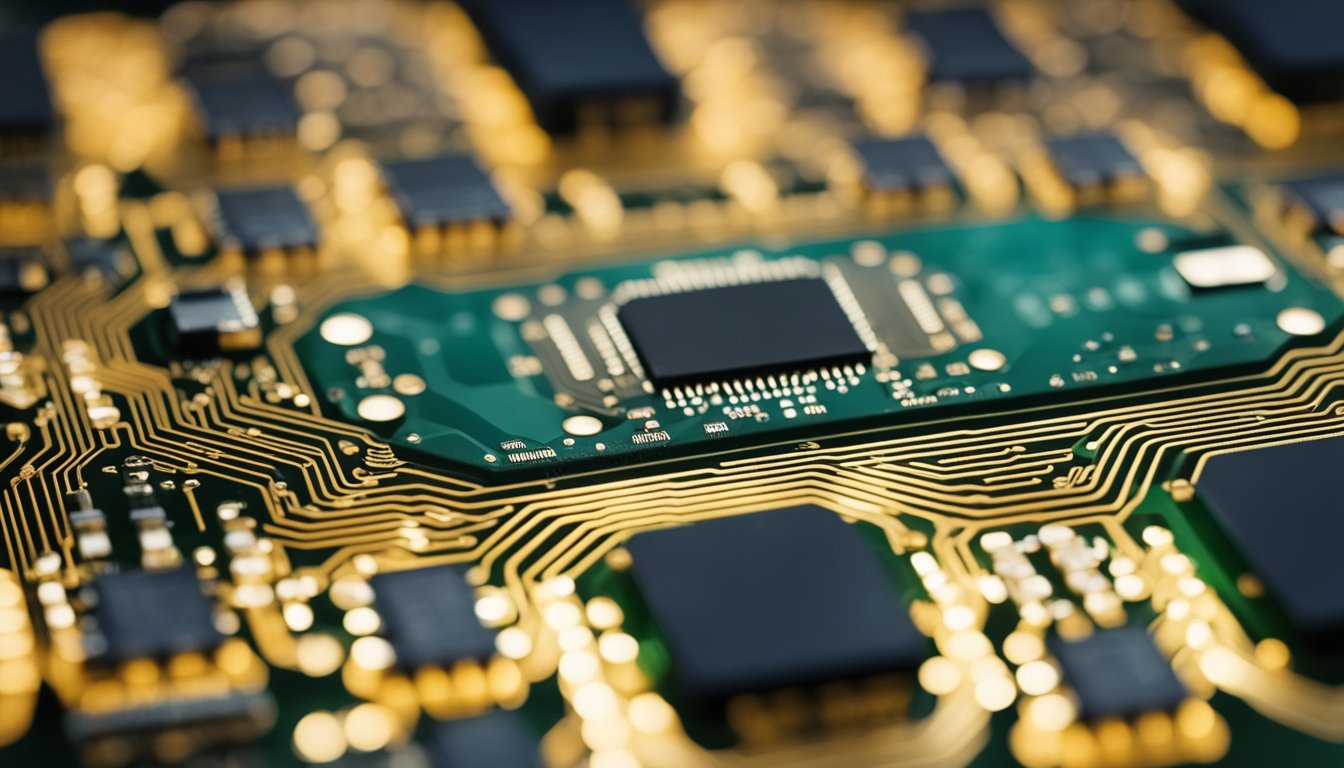
Membrane PCB is a type of printed circuit board that is flexible and can be used in a wide range of applications. They are made up of several layers of material, including a flexible substrate, conductive traces, and a protective layer. The flexibility of the substrate allows for a greater degree of design freedom, making it possible to create custom shapes and sizes.
One of the key advantages of membrane PCBs is their low profile, which makes them ideal for use in devices where space is at a premium. They are also lightweight and durable, making them suitable for use in harsh environments. In addition, membrane PCBs are highly customizable, allowing for a wide range of design options.
A membrane PCB is a type of switch that consists of a printed circuit board (PCB) and a flexible membrane layer. The membrane layer is typically made of polyester or polycarbonate, and it contains conductive traces that are used to create a circuit when pressure is applied to the top layer. Membrane PCBs are commonly used in products that require a low-profile and lightweight design, such as medical devices, consumer electronics, and industrial equipment.
One of the main advantages of membrane PCBs is their durability. Since there are no moving parts, they can withstand a high number of actuations without wearing out. Additionally, they are resistant to moisture, dust, and other contaminants, which makes them ideal for use in harsh environments.
Membrane PCBs are made up of several components, including the membrane layer, the PCB layer, and the adhesive layer. The membrane layer is typically made of a thin, flexible material that is printed with conductive traces. The PCB layer is a rigid board that is used to support the membrane layer and provide a stable base for the switch. The adhesive layer is used to bond the two layers together.
The materials used to make membrane PCBs are carefully chosen to ensure that they are both durable and reliable. The membrane layer is typically made of polyester or polycarbonate, which are both strong and flexible materials that can withstand repeated use. The conductive traces are usually made of silver or copper, which are both highly conductive metals that can carry electrical signals with minimal resistance. The adhesive layer is typically made of acrylic or silicone, which are both strong and flexible materials that can withstand a wide range of temperatures and environmental conditions.
In summary, membrane PCBs are a type of switch that combines a printed circuit board with a flexible membrane layer. They are durable, reliable, and ideal for use in products that require a low-profile and lightweight design. The components and materials used to make membrane PCBs are carefully chosen to ensure that they are both durable and reliable.
When designing a membrane PCB, there are several factors to consider to ensure that the final product meets the desired requirements. The following subsections outline some of the most important design considerations.
The electrical layout is a critical aspect of membrane PCB design. The layout must be carefully planned to ensure that the circuitry is precise, fast, and accurate. A good electrical layout should also minimize noise and interference to ensure that the device operates reliably.
When designing the electrical layout, consider the following factors:
In addition to the electrical layout, the mechanical constraints of the membrane PCB must also be considered. The mechanical design should be optimized for the intended use of the device and should take into account factors such as durability, flexibility, and ease of use.
When designing the mechanical constraints, consider the following factors:
By carefully considering these design considerations, you can ensure that your membrane PCB meets the desired requirements and operates reliably over its intended lifespan.
Membrane PCBs are a type of flexible printed circuit board that is used in various electronic devices. These PCBs are made up of a thin, flexible polymer film that is laminated with a conductive metal layer. The manufacturing process of membrane PCBs involves several steps, including printing technologies, layer stacking, and sealing.
The first step in the manufacturing process of membrane PCBs is the printing of the conductive metal layer on the polymer film. There are several printing technologies used for this purpose, including screen printing, offset printing, and digital printing. Screen printing is the most commonly used technology for printing the conductive layer on the polymer film. This technology involves the use of a fine mesh screen that is stretched over a frame. The screen is coated with a photosensitive emulsion, and the design of the circuit is printed on the screen using a film positive. The screen is then exposed to light, which hardens the emulsion on the screen in the areas where the circuit design is printed. The unhardened emulsion is then washed away, leaving behind a stencil that is used to print the conductive ink onto the polymer film.
Once the conductive metal layer is printed on the polymer film, the layer stacking process begins. In this process, several layers of the polymer film are stacked on top of each other, with each layer having a different conductive metal layer printed on it. The layers are then aligned and bonded together using an adhesive. The adhesive used in this process is typically a pressure-sensitive adhesive that is activated by heat.
After the layer stacking process is complete, the membrane PCB is sealed to protect it from environmental factors such as moisture and dust. The sealing process involves the use of a protective film that is laminated onto the surface of the PCB. This film is typically made of a polymer material that is resistant to moisture and dust. The film is then trimmed to the desired size and shape of the PCB.
In conclusion, the manufacturing process of membrane PCBs involves several steps, including printing technologies, layer stacking, and sealing. The use of these technologies ensures that the membrane PCB is flexible, durable, and resistant to environmental factors.
Membrane PCBs are widely used in various industries due to their low profile, flexibility, and durability. Here are some of the most common applications of membrane PCBs:
Membrane PCBs are widely used in consumer electronics, such as mobile phones, tablets, and remote controls. These devices require a low profile and durable interface that can withstand repeated use. Membrane PCBs are an ideal solution for such applications due to their flexibility and low profile. They can be customized to fit the exact specifications of the device, and they offer an excellent tactile response.
Membrane PCBs are also used in medical devices, such as blood glucose monitors, heart rate monitors, and infusion pumps. These devices require a sterile and durable interface that can withstand repeated use. Membrane PCBs are an ideal solution for such applications due to their ability to be easily cleaned and sterilized. They can also be customized to fit the exact specifications of the device, and they offer an excellent tactile response.
The automotive industry is another sector that utilizes membrane PCBs. These devices are used in various applications, such as dashboard controls, climate control systems, and audio systems. Membrane PCBs are an ideal solution for such applications due to their low profile and durability. They can also be customized to fit the exact specifications of the device, and they offer an excellent tactile response.
In conclusion, membrane PCBs are widely used in various industries due to their flexibility, low profile, and durability. They are an ideal solution for applications that require a sterile and durable interface that can withstand repeated use. Membrane PCBs can be customized to fit the exact specifications of the device, and they offer an excellent tactile response.
One of the main advantages of using membrane PCBs is their durability and flexibility. Membrane PCBs are made of thin, flexible materials that can withstand bending and twisting without breaking. This makes them ideal for use in applications where the PCB needs to be flexible, such as in medical devices or wearable technology. Additionally, the flexibility of membrane PCBs allows for more compact designs, which can be beneficial in applications where space is limited.
Another advantage of membrane PCBs is their cost-effectiveness. Because they are made of thin, flexible materials, membrane PCBs can be produced using less material than traditional PCBs. This means that they can be produced at a lower cost, which can be beneficial for companies looking to reduce manufacturing costs. Additionally, because membrane PCBs are thinner and more flexible, they can be produced in larger quantities and at a faster rate than traditional PCBs.
While membrane PCBs offer many advantages, they also come with some design limitations. Because they are made of thin, flexible materials, membrane PCBs are not suitable for all applications. For example, they may not be able to handle high power or high-speed signals, which can limit their use in certain applications. Additionally, because of their flexible nature, membrane PCBs may not be suitable for applications where the PCB needs to be rigid and stable.
In summary, membrane PCBs offer many advantages, including durability, flexibility, and cost-effectiveness. However, they also come with some design limitations that must be considered when choosing the appropriate PCB for a specific application.
Do you have any questions, or would you like to speak directly with a representative?